We use cookies to make your experience better. To comply with the new e-Privacy directive, we need to ask for your consent to set the cookies. Learn more.
JTAG/SWD debug probe with USB interface
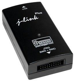
J-Link PLUS is a USB powered JTAG debug probe supporting a large number of CPU cores. Based on a 32-bit RISC CPU, it can communicate at high speed with the supported target CPUs. J-Link is used around the world in tens of thousand places for development and production (flash programming) purposes.
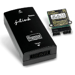
J-Link PLUS is available in two form factors with identical function: J-Link PLUS and J-Link PLUS Compact.
The J-Link debug probes are supported by all major IDEs including Eclipse, GDB-based IDEs and SEGGER Embedded Studio. For a complete list, please refer to Supported IDEs. Including all models, more than 500,000 J-Links have been shipped so far, making J-Link probably the most popular debug probe for ARM cores and the de-facto standard.
Media
Licensing
J-Link PLUS comes with licenses for all J-Link related SEGGER software products:
J-Link Unlimited Flash Breakpoints, J-Link RDI / RDDI, J-Flash providing the optimum debugging experience for professional developers.
- Comes with integrated licenses for: Unlimited breakpoints in flash memory (Unlimited Flash Breakpoints), RDI / RDDI and J-Flash
- Superset of J-Link BASE [More..]
- Supports a broad range of microcontrollers [More..]
- Supports direct download into RAM and flash memory
- Download speed up to 1 MByte/s
- Supports unlimited breakpoints in flash memory [More..]
- Multiple CPUs supported—8051, PIC32, RX, ARM7/9/11, Cortex-M/R/A, RISC-V [More..]
- Free software updates
- Built-in VCOM functionality [More..]
| Specification | Value | ||||
|---|---|---|---|---|---|
| Supported OS | Microsoft Windows 2000, XP, 2003, Vista, 7 and newer (32 bit and 64 bit versions) Linux macOS 10.5 and higher | ||||
| Electromagnetic compatibility (EMC) | EN 55022, EN 55024 | ||||
| Operating temperature | +5°C ... +60°C | ||||
| Storage temperature | -20°C ... +65 °C | ||||
| Relative humidity (non-condensing) | Max. 90% rH | ||||
| Mechanical | |||||
| Size standard housing (without cables) | 100mm x 53mm x 27mm | ||||
| Weight standard housing (without cables) | 70g | ||||
| Size compact device (without cables) | 47mm x 40mm x 14mm | ||||
| Weight compact device (without cables) | 20g | ||||
| Available Interfaces | |||||
| USB interface | USB 2.0 (Hi-Speed) | ||||
| Target interface | JTAG/SWD 20-pin (adapters available) | ||||
| JTAG/SWD Interface, Electrical | |||||
| Power supply | USB powered Max. 50mA + Target Supply current. | ||||
| Target interface voltage (VIF) | 1.2V ... 5V | ||||
| Current drawn from target voltage sense pin (VTRef) | < 25µA | ||||
| Target supply voltage | 5V (derived from USB voltage) | ||||
| Target supply current | Max. 300mA | ||||
| Reset type | Open drain. Can be pulled low or tristated | ||||
| Reset low level output voltage (VOL) | VOL <= 10% of VIF | ||||
| For the whole target voltage range (1.2V <= VIF <= 5V) | |||||
| LOW level input voltage (VIL) | VIL <= 40% of VIF | ||||
| HIGH level input voltage (VIH) | VIH >= 60% of VIF | ||||
| For 1.2V >= VIF <= 3.6V | |||||
| LOW level output voltage (VOL) with a load of 10 kOhm | VOL <= 20% of VIF | ||||
| HIGH level output voltage (VOH) with a load of 10 kOhm | VOH >= 80% of VIF | ||||
| For 3.6 <= VIF <= 5V | |||||
| LOW level output voltage (VOL) with a load of 10 kOhm | VOL <= 20% of VIF | ||||
| HIGH level output voltage (VOH) with a load of 10 kOhm | VOH >= 80% of VIF | ||||
| JTAG/SWD Interface, Timing | |||||
| Target interface speed | Max. 15 MHz | ||||
| SWO sampling frequency | Max. 30 MHz | ||||
| Data input rise time (Trdi) | Tfdi <= 20ns | ||||
| Data output rise time (Trdo) | Trdo <= 10ns | ||||
| Data output fall time (Tfdo) | Tfdo <= 10ns | ||||
| Clock rise time (Trc) | Trc <= 3ns | ||||
| Clock fall time (Tfc) | Trc <= 3ns | ||||
Tecnologix offers support which is directly handled by development team. Do not hesitate to get in touch with our experts.
Just ask here


